Micro Manufacturing at Rocket Scream
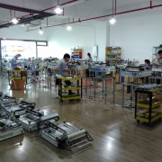
In the past 2 months, we were in manufacturing mode churning out boards like osPID Kit, TraLog Shield, and Reflow Oven Controller Shield. About 400 boards were assembled in our secret lab within this period and we thought it would be cool to share with everyone on how we went through the whole micro manufacturing process.
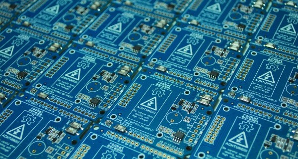
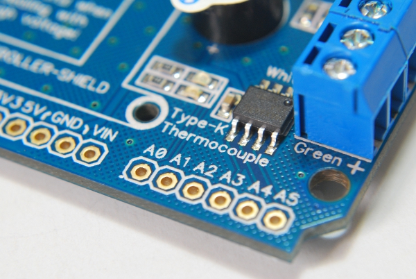
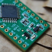
We usually have our bare PCB boards in single pieces rather than in a panel as we don’t have a pick and place machine. Furthermore, we don’t really like the uneven edge when v-score lines are used in a PCB panel. We usually stick to immersion gold as our preferred surface finish due to it’s very flat surface although it costs more than other PCB surface finish (HASL, immersion silver).
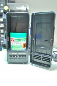
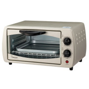
The process of assembling the boards are usually split into 2 stages. We would first assemble the surface mount components using the reflow oven toaster method before manually assembling the through hole components. When we first started, we used solder paste in a syringe and dispensing them dot by dot on the pads of a PCB. This is a very slow and painstaking process. When we started making more boards, we move to solder paste in a jar. But, you’ll need to keep the solder paste in a proper storage to avoid the solder basically from drying off. We used a simple USB mini fridge to do this.
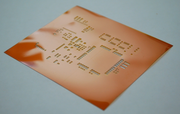
You’ll need a stencil to apply the solder paste onto your PCB. We got ours from Ohararp and we think their service is awesome. After so many boards assembled, the stencil still can be reused without any solder paste smearing issues. We think that Kapton based PCB stencil are more suitable for small scale manufacturing due to it’s small size. We’ll definitely move on to metal based stencil once we move into automated assembly in factory.
The setup below is usually how we dispense our solder paste onto the PCB. It’s best to leave a small gap (enough for 1 finger) on one of the PCB side which can be used to lift the PCB up once the solder paste has been applied.
Once we got the stencil frame setup completed, we’ll stick one side of the stencil onto the PCB after aligning them to the pads on the PCB. We left the opposite site of the stencil unattached to allow us to easily lift the stencil up once the process is complete.
We used a thin squeegee bought from a hardware shop to apply the solder paste. A good practice would be cleaning the bottom side of the stencil after 3 boards with a kitchen towel to avoid any solder paste leftover on unwanted area of the PCB.
If an automated pick and place machine like Luna 7722 has a 54 tape feeders, we probably have more feeders than that! In order to make the process of picking and placing faster, we used ice cube trays to organize our components. Each cube location is labelled to indicate the component type and the corresponding component reference designator. Each of the ice cube tray can be used for a different PCB by placing the labels on 4 different cube walls. By doing this, you don’t have to peel off the labels every time you have a different board to assemble. A good practice of the components placement in the ice cube tray would be placing similar components types far away from each other. For example, 0603 1 μF & 100 nF ceramic capacitor looks exactly the same. It would be disastrous if you mistakenly mix them up. By placing them far apart (and in between other type of components), you will most probably avoid putting yourself in that mix-up situation. On top of that, it would be a good advantage if you can understand some of the components markings like what is 103 means on a SMD resistor. Lastly, it is best to tape the bottom of the ice cube tray to the table to avoid them from flipping over and looking at a pile of mix-up components (experience speaks for itself)!
In order to easily identify which component to place on the PCB, we usually print out an enlarged copy of the PCB layout (only component silkscreen and pads are required). But, once you started to pick and place for quantities more than your fingers can count, you can easily remember all the component type and values!
Now all you need is a sharp pair of tweezers and a cup of coffee to get you going! Once we completed the pick and place process for the SMD components, we tossed the boards into our reflow oven and let our Reflow Oven Controller Shield to do the rest of the work. This is the result we usually get from the reflow process:
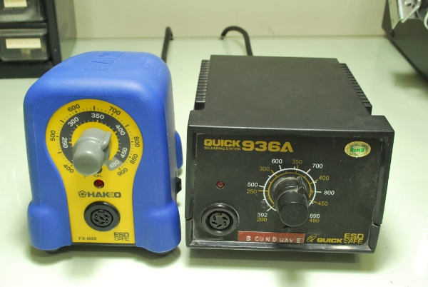
After we have completed the SMD components assembly process, we let all the boards to cool down. The next step is to manually solder the remaining through hole components (if any) onto the boards. Lead-free soldering is not as easy as leaded soldering. We use a Hakko FX-888 and also a Hakko 936A (ours is an imitation version!) to do the manual soldering.
We used 2 sets of solder spool with different diameter:
We usually use the 0.6 mm solder when the pads on the PCB is smaller (example: 2.54 mm pitch connectors) and the 0.7 mm solder when the pads on the PCB is larger (example: terminal blocks, relays). By choosing the correct solder diameter size, we spent less time heating up the pad (which is better for the components) as lead-free soldering takes place at higher temperature. We prefer the Asahi 0.6 mm solder over the Multicomp 0.7 mm solder (smell maybe?). Despite the no-clean claims, we usually still have some residue left on the PCB after the manual soldering process. We used Kontakt PCC printed circuit board cleaner to remove the residue and we think they are best PCB cleaner around (we used a whopping 4 cans of Kontakt within 2 months!).
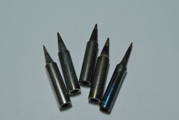
One of the problem that we faced during lead-free soldering is the oxidization process of the solder tip which happens at a much faster rate compared to leaded soldering. This is due to the higher temperature requirement of the lead-free soldering process. Once the tip becomes oxidized, the solder tip becomes less efficient and you’ll spent more time getting the solder to meld. Just look at how many solder tips being used during the entire assembly process! Each of these Hakko solder tips cost about USD5-6 (depending on solder tip size).
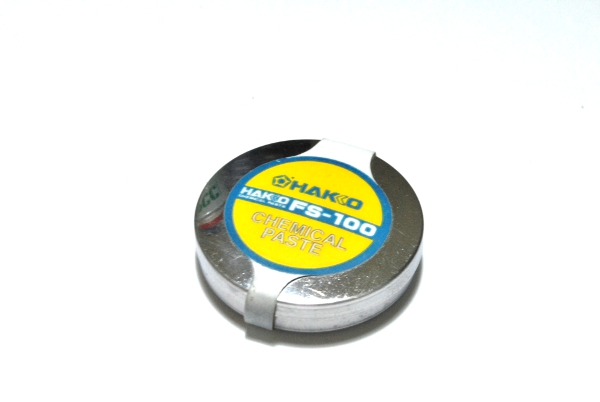
We found that Hakko FS-100 Chemical Paste helps to pro-long your tip lifespan. By dipping your hot solder tip into the paste, the tips gets shinny and new again. But, after some time, you’ll notice the solder tip wouldn’t be able to react positively to the chemical paste anymore.
Once the PCB cleaning process is completed, we move on to test the boards and seal-packed them in anti-static bags!
We shall leave the packing and shipping process into another post!
We hope you enjoy reading and take care!







Where did you fabricate your PCB? its look nice.
Azri,
We got them made by Circuit Mart.
Awesome folks!